 Multiplexor Problem
This was where I first really walked into a wall not knowing what I was doing. I had designed and built the first simple gates (2 input AND, OR and XOR) and thought I would try to do the logic part of the ALU. This was going to be simple. For each bit of the logic unit I'd have a set of simple gates (ie an AND, an OR and an XOR) feeding a 3:1 multiplexor.
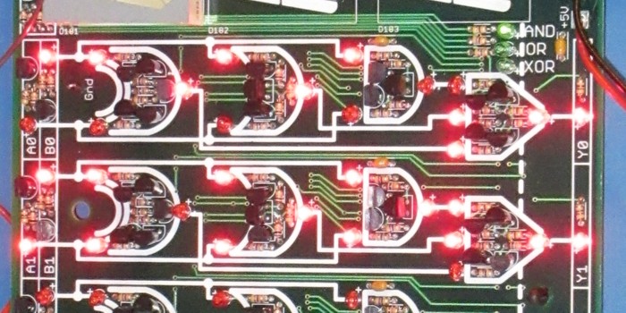
The initial test of the finished board was promising, here are some pictures where I've set up an input of 0x00 and 0x01 and am going through the mutiplexor options.
| 0x00 AND 0x01 | 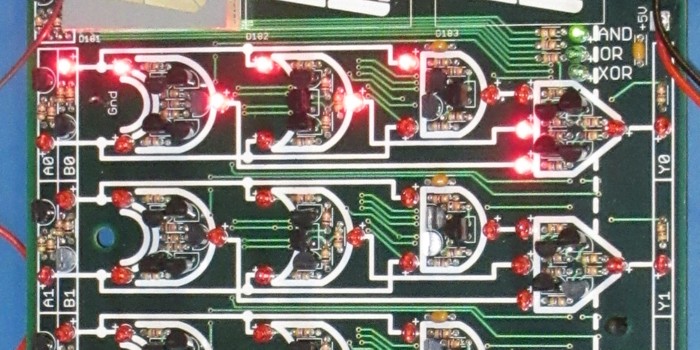 |
| 0x00 OR 0x01 | 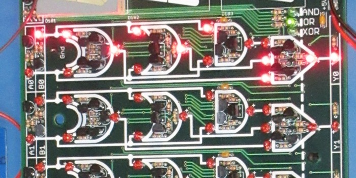 |
| 0x00 XOR 0x01 | 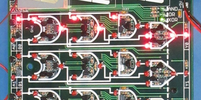 |
So far so good. But it all started going wrong when things started happening on other bits:
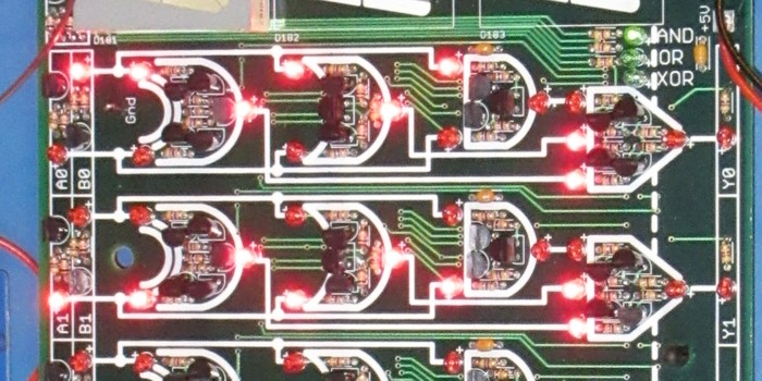
| Doing 0 AND 1 on bit 0, Doing 1 AND 0 on bit 1, ....everything is fine |
 |
| Doing 0 AND 1 on bit 0, Doing 1 AND 1 on bit 1, ...bit 0 is incorrectly outputting 1 |
 |
On investigation I discovered that if any output multiplexor of the logic unit should output a 1 then all output multiplexors that had any inputs set to 1, whether selected or not, would also output a 1.
I really struggled to understand what was going on.
The relevant fragment of the schematic is:
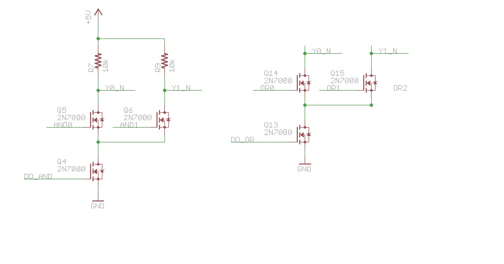
When designing this I believed that if DO_OR was low then Q13 would not be conducting and therefore the values of OR0 and OR1 would be irrelevant regardless of what else was happening. Turns out that was incorrect. It took me ages to work out what was happening but eventually it dawned on me that there must be some kind of "reverse" path possibly/probably involving the body diode of the FET.
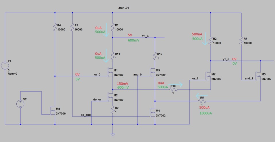
I've just now finally got round to looking at it in simulation. The schematic below is what I put into Spice and is equivalent to the schematic fragment above. V2 provides a pulse so I can see what happens as OR0 changes and I've annotated the schematic with the voltages/currents when OR0 is in its two states, "0" in red, "1" in green. (The 1? resistors are just to make it easier for me to see the current in Spice). I was correct in that Q13 of the original schamtic (M2 in the one for Spice) does not conduct either way. What I missed was that when OR0 is on and Q14/M1 can conduct there is an alternate path for the current going through the body diode of Q14/M7 which means that y0_n is pulled low. Because of the body diode in the path y0_n can't go as low as y1_n and drops to only 600mV which corresponds to the voltage drop across the diode.
Even though I now know this happens I still find it very difficult. Back then I struggled even more so I was very cautious when I next tried to design a multiplexor. That next design worked and I've stuck with it. The downside is that I think it's probably overcautious and I've ended up soldering a lot more transistors than needed.
- Home
- Vital Statistics
- Progress
- Architecture
- Stepping Stones
- Programming
- Peripherals
- Construction
- Cost & Materials
- Good, Bad & Ugly
- History
- Build Faults
- Flip Flops
- Modelling
- Architecture Choice
- Logic Type
- 7 segment
- Board Shape
- Dual Output
- ALU
- SRAM
- Speed
- Speed 2
- Buses
- Area
- Efficiency
- LED supply
- Multiplexor Problem
- Multiplexor Errors
- Surface Mount
- Solder
- Health & Safety
- Web
- Links
- Contact

© 2014-2016 James Newman.