 Modules
This is a gallery of the modules that make up the Megaprocessor.
State Machine
The state machine controls the operation of the processor; directing the execution of each instruction.
Artwork files (Eagle schematic & board, pdf version).
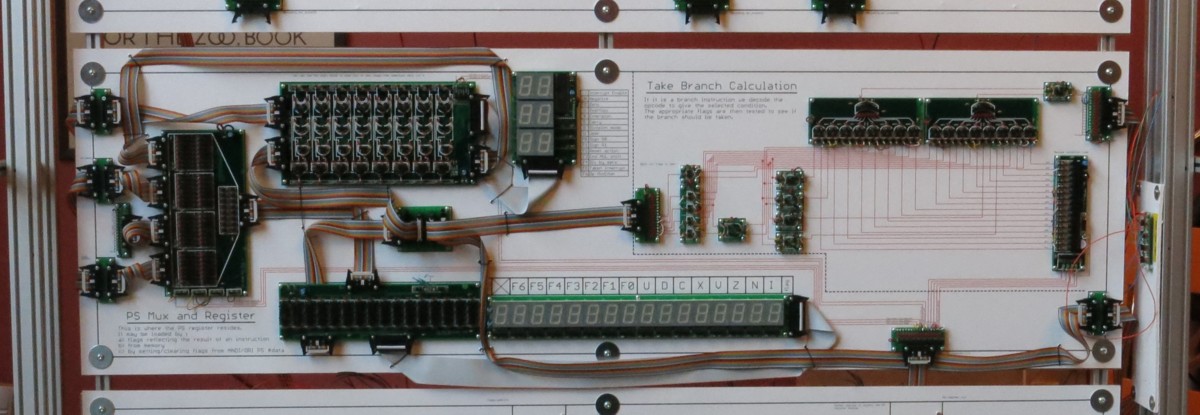
Status Register
The status register is a collection of bits that record various
aspects of the results of previous calculations. Whilst PS is
internally a 16 bit register only 8 bit are visible to the user,
the other hidden 8 bits are used during complex operations such
as multiplication etc. and do not convey any information from
one instruction to the next. The status bits are:
Artwork files (Eagle schematic & board, pdf version).
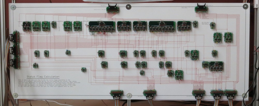
Flag Calculation
The status flags are calculated using the results generated by various parts of the processor, in particular the ALU, depending on the instruction being executed. They are stored in the status register.
Artwork files (Eagle schematic & board, pdf version).
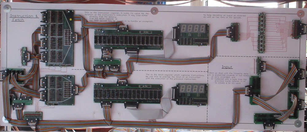
Fetch & Instruction
The current instruction is stored here. In addition if the next
instruction has been fetched before it is needed (which usually
occurs during load/store instructions) it is stored here in its
own register (F) till needed. During exception processing the
TRAP instruction is generated here and inserted directly into
the instruction register.
Also the read data arrives here and is passed onwards in two forms, zero extended, and combined with a previously read byte held in H to form a 16 bit value.
Artwork files (Eagle schematic & board, pdf version).
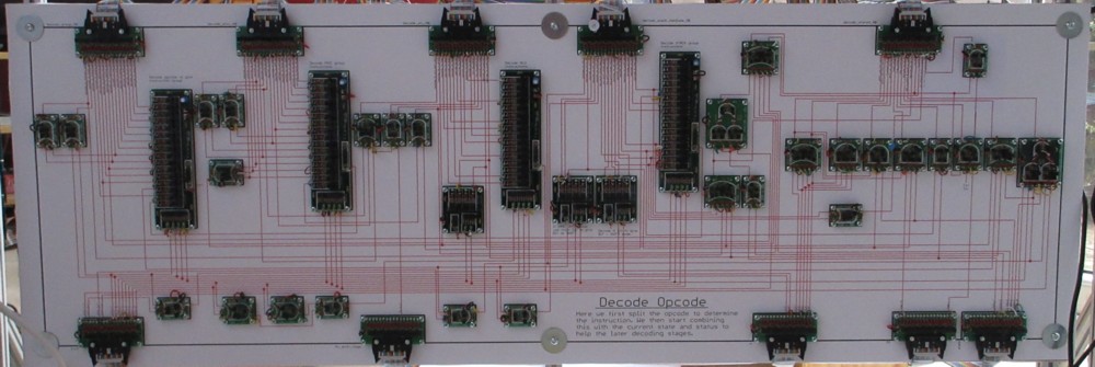
Opcode Decode
This decodes the opcode to work out what the instruction is.
Artwork files (Eagle schematic & board, pdf version).
Decode A
This bundles together signals from the Opcode Decode module for
routing to other modules. In particular the State and Special
Purpose Control modules. As well as routing it also generates
some signals required by both those modules to begin the task of
working out what needs to be done this cycle.
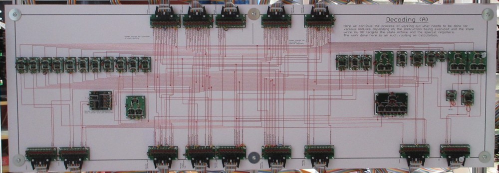
Artwork files (Eagle schematic & board, pdf version).
Decode B
This bundles together signals from the Opcode Decode module for
routing to other modules. In particular the Status Flags
Calculation, ALU Control and Rnx Control modules. As well as
routing it also generates some signals required by both those
modules to begin the task of working out what needs to be done
this cycle.
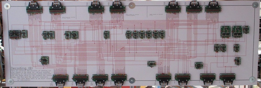
Artwork files (Eagle schematic & board, pdf version).
Special Purpose Registers
This is where the processor registers Stack Pointer (SP),
Program Counter (PC) and Helper (H) registers are. In addition
the registers driving the external address bus and write data
are here. Most of the functionality is just multiplexing but
there is also an adder provided to allow the H register count
out the number of iterations required for iterative
instructions.
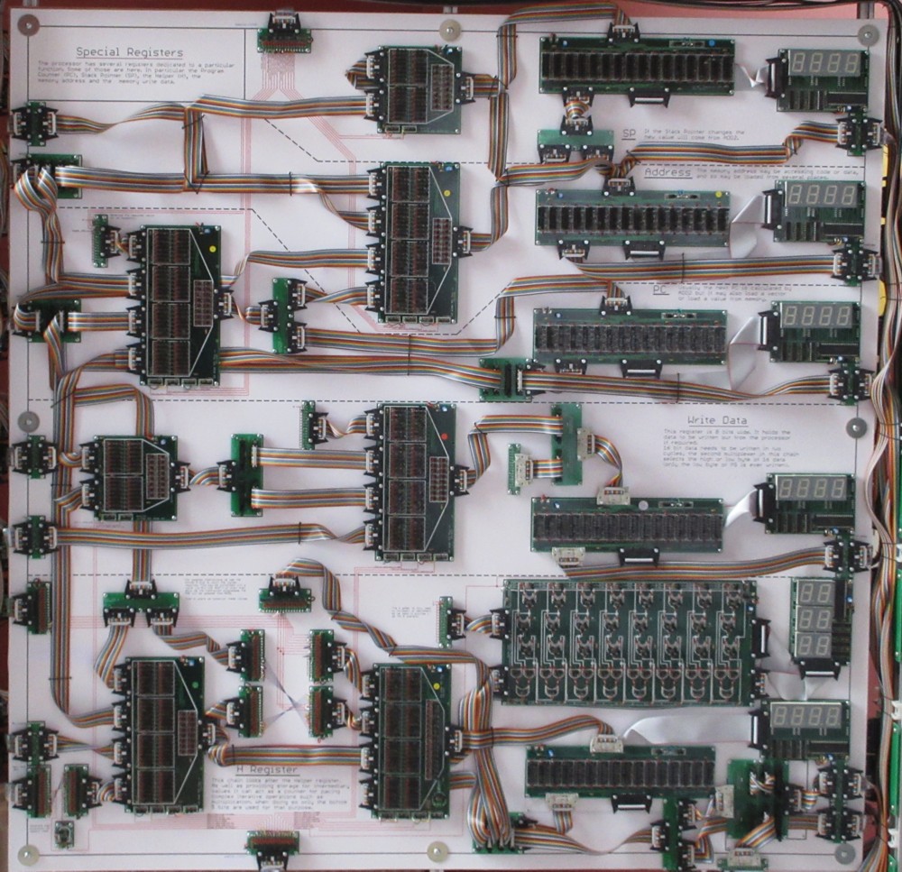
Artwork files (Eagle schematic & board, pdf version).
Special Registers Control
This module generates the control signals for the Special
Purpose Registers module. To do this it uses information from
the decoder modules together with current state (and also the
count in H for iterative instructions) to work out what needs to
be done this cycle.
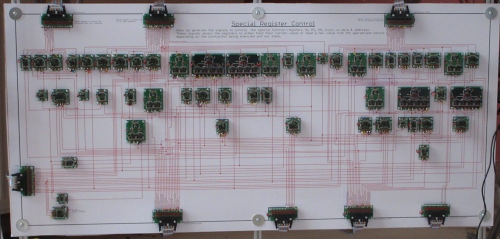
Artwork files (Eagle schematic & board, pdf version).
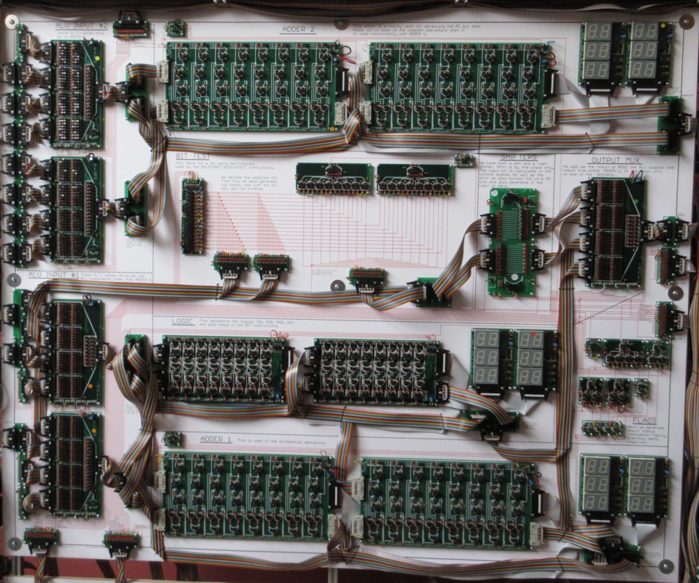
ALU
This is where the arithmetic and logical operations are carried out. It splits into two parts ALU1 and ADDER2. Each have two inputs, X and Y.
ADDER2 is much the simpler consisting only of a 16 bit adder/subtractor.
ALU1 has several computational units, a 16 bit
adder/subtractor, 16 bit logic, left and right shifters, logic
for the BIT operations. The result from only one of these is
output. Flags reporting various aspects of the results (zero,
negative, overflow) are sent to the Status Flags
Calculation module.
Artwork files (Eagle schematic & board, pdf version).
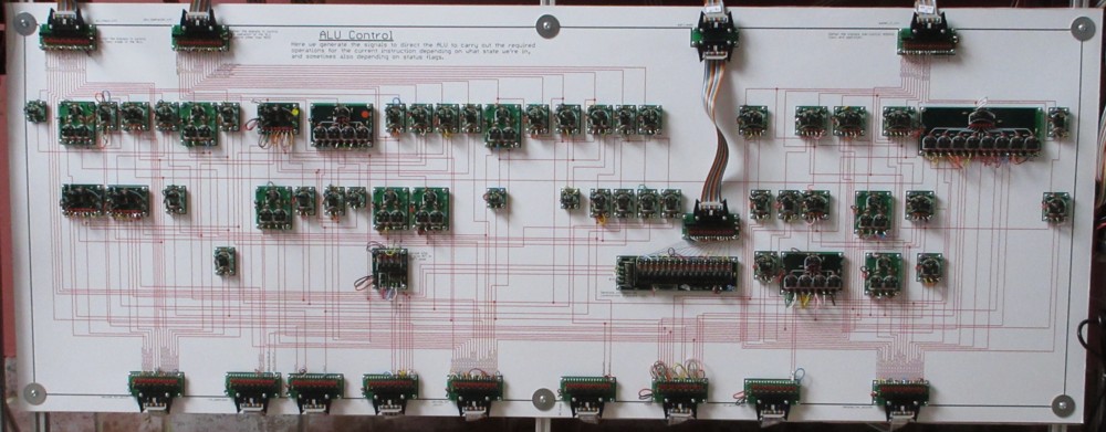
ALU Control
This module generates the control signals for the ALU module. To do this it uses information from the decoder modules together with current state, the current status and the H register (for SHIFT and BIT) to work out what needs to be done this cycle. It also generates the sequence of values required for the SQRT algorithm.
Artwork files (Eagle schematic & board, pdf version).
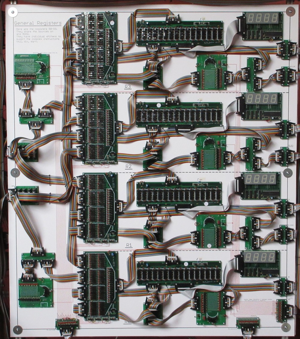
Rn Registers
This is where the General Purpose Registers (R0, R1, R2, R3) live. They can be written to from various places.
Usually at most one register is written to in a cycle. However
during MUL and DIV upto all 4 may be written to in a cycle. In
this mode each register has its own shifter to generate its
required new value.
Artwork files (Eagle schematic & board, pdf version).
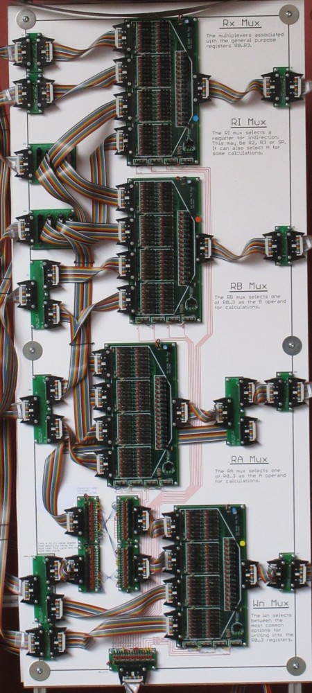
Rx Mux
This multiplexes R0:R3 to generate three buses (RA, RB and RI)
that act as sources for operations. It also multiplexes several
buses to generate the Wn bus that may be used as one of the
results that can be written into the R0:R3 registers.
Artwork files (Eagle schematic & board, pdf version).
Rnx Control
This generates the signals that control what the Rn Registers
and Rx Mux modules do each cycle. This depends on the current
state and instruction and uses signals generated by the decoder
modules.
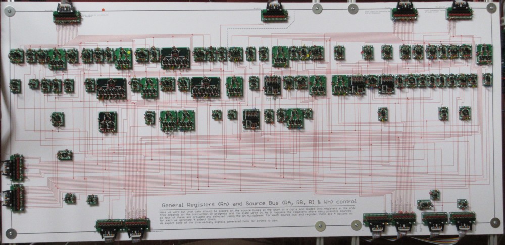
Artwork files (Eagle schematic & board, pdf version).
© 2014-2016 James Newman.
