 Modelling
This I think worked well. If the project is a success then this will be one of the key reasons.
Once I realised that I had decided to build a processor I took a bit of time to think about how I should go about it. And whilst I could see many problems it seemed to me that there was one that was certainly the biggest of all. How could I be sure that what I built was what I had designed ?
The particular reason why I was nervous was because the processor was going to be built by connecting together lots of small boards and there was plenty of scope for errors at all stages. When sensible people build a processor nowadays the design they come up with is translated directly to hardware. There may be some manual tweaks on the way but the translation is essentially mechanical and so (we trust) reliable. (There are languages specifically for describing hardware designs e.g. Verilog and VHDL). By contrast once I'd designed the processor I was then going to build it using a completely independent process.
So the first decision was that when I started to physically build the processor there had to be a route by which I could test it at each stage against the design. So each individual board, each collection of boards into modules, each collection of modules etc.would be tested against the appropriate subset of the design. This led me to using a general purpose language (C/C++) to describe the design so that exactly the same software that was used to design (model) the processor could be incorporated without modification into a test system.
Obviously if the software model of the processor is to be used to test any part of the processor it must represent it exactly in terms of its lowest level gates.
But to design a processor from gates up would be an exercise in misery. Very fiddly and quite difficult to be sure you'd got it right.
So I first designed the processor in a quite abstract way without any real consideration as to the implementation; modelling it as a set of instructions acting on a group of registers. This is a really easy way to describe it which has the benefit that there is some chance I might get it right. For example here is the business part of the ADD instruction
void clDecodeADD::Execute(clEmuRegSet * pReg, clEmulatorMemAccess * pAccess)
{
unsigned short origA, origB;
(void) pAccess;
// op
origA = pReg->m_aReg[m_A];
// need to catch original values of A&B for flag
calculation
origB = pReg->m_aReg[m_B];
pReg->m_aReg[m_A] += pReg->m_aReg[m_B];
// flags
EMU_SetFlagsAdd(pReg->m_aReg[EMU_REG_PS], origA, origB, pReg->m_aReg[m_A]);
}
Once I had an abstract model of the processor that I was happy with I then set about modelling how it could be implemented in hardware using logic gates. To check that the hardware model was correct I would run it in parallel with the abstract model on the same programs/data and check they moved in lock step with each other. For an example of what the hardware model looks like here is a fragment that is modelling the logic to control the multiplexer feeding the Y input of the ALU.
// ALU1 Y
alu1_y_mux_RB_A = Cpnt_8OR(bus_decode_alu_2.opcode_is_and_group,
bus_decode_alu_2.opcode_is_or,
bus_decode_alu_3.opcode_is_xor_group,
bus_decode_alu_3.opcode_is_mover,
bus_decode_alu_2.opcode_is_add_group,
bus_decode_alu_3.opcode_is_sub_group,
bus_decode_alu_3.opcode_is_cmp_group,
bus_rnx_specials.adder_y_special);
alu1_y_mux_RB = Cpnt_3OR(alu1_y_mux_RB_A,
bus_decode_alu_2.opcode_is_shift_xx,
bit_xx_load_cycle);
alu1_y_mux_k = Cpnt_4OR(bus_decode_alu_3.opcode_is_addq_group,
bus_decode_alu_3.opcode_is_stack_group,
bus_state[STATE_MAIN_MULTIPLY],
bus_PS[WiC_PS_FLAG_INDEX_F3]);
alu1_y_mux_bit = Cpnt_2AND(bit_xx_action_cycle,
~bit_shift_mode_decode.Output()[BIT_SHIFT_MODE_CLEAR]);
alu1_y_mux_not_bit = Cpnt_2x2AND_OR(bit_xx_action_cycle, bit_shift_mode_decode.Output()[BIT_SHIFT_MODE_CLEAR],
bus_decode_alu_3.opcode_is_inv, bus_decode_alu_3.opcode_is_inv);
By keeping the abstract model as a reference I could experiment with the hardware model trying out different approaches confident that if its behaviour matched that of the abstract model then it would yield a working processor.
Having fixed on a hardware design (modelled by a software program) the next step was to create the schematics for the modules. I desperately wanted to find a mechanical way of going from the software program to the schematic but couldn't find a satisfactory way of doing that. So I copy and pasted the program into a schematic as comments and for each gate of the design matched up the symbol for the board implementing it with the function call in the software program that modeled it. Then it was a matter of labeling all the signals as per the variables in the software program. The result for the above fragment is shown below:
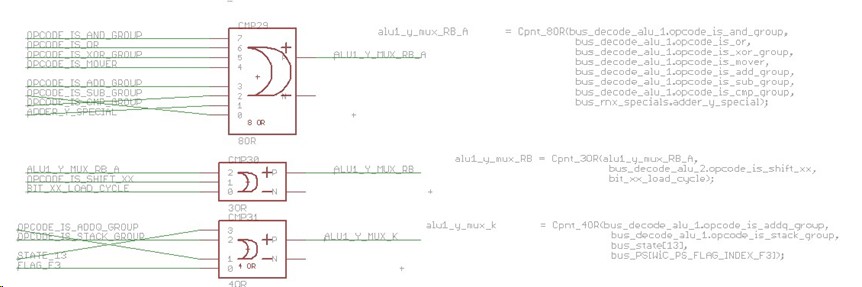
Once I'd done that I could use a PCB layout design tool to translate the schematic into the artwork I used for the modules. This artwork is what I used to tell me how to wire things together. The PCB tool ensures that the artwork is consistent with the schematic (which is hopefully consistent with the hardware model, which is consistent with the abstract model, and so will result in a working processor ). (You may be puzzled by the apparently random crossing of some of the lines in the picture above. When I initially drew the schematic it was neater, for example STATE_13 connected to input #1 of the OR gate at the bottom, and OPCODE_IS_ADDQ_GROUP connected to #3. When "laying out" the artwork I found it more convenient to have these swapped round, which is perfectly legal todo as all inputs to an OR gate are equivalent. So I swapped them in the layout and the tool ensures they are swapped in the schematic to maintain consistency. A process called back-annotation. However it doesn't care about aesthetics so doesn't do anything to straighten the lines or move the labels. I don't manually prettify it again in case I mess up, its not worth the risk)
Each time I connect some boards together to form part of the processor I run a test on it. The test program incorporates the matching part of the hardware model and so can run the hardware in parallel with the model and check they move in lock step with each other. This way I have a chain of verification from the hardware back to my abstract model, which is the reference definition.
As well as acting as a reference for the design the abstract model also sees service in the simulator.
If I had my time again what would I change?
- I dithered for some time as to whether I should use one of the hardware description languages (I'd have probably chosen VHDL) to describe my hardware model, it's what they're designed for after all. Towards the end of the project I did in fact create a VHDL version of the processor. This was so that I could run a version in an FPGA for testing parts of the system. (I did this by renaming my *.CPP files to *.VHD and then sorting out the compilation errors. Literally). However I'm still pretty sure that it was correct to use software for the modelling. The crucial factor is being able to run the exact same model in the test program but also software provides a much more benign environment for experimenting with ideas.
- The bit I would most like to have changed was the manual translation from the hardware model to schematic. If I had my time again I think I'd look very hard for a way of avoiding this. Perhaps/probably by having some third form of description from which I could automatically generate both the software and the schematic (and probably the VHDL as well). I'm sure its possible, the mistake I made was to write the software model first and then wonder how to turn it into a schematic by which time it was too late.
- The other thing I'd like to have done is create a graphical simulator using the same artwork as I used for the modules. Complete with flashing LEDs. This may well have easily fallen out if I'd properly solved the software/schematic translation. I do find myself gnawing on this every now and then and think it's not so hard. If I had done this then a rather fun idea a friend suggested was that you could use an image processing approach to test. Train a camera on the Megaprocessor as it runs and check its lights flash in the same places as on the simulator. Bonkers. But fun. Whilst its too late to have automatically created the artwork I think its reasonably straightforward to go from the artwork to a graphical simulator, so there might be a virtual Megaprocessor arriving in a while.
- Home
- Vital Statistics
- Progress
- Architecture
- Programming
- Peripherals
- Construction
- Cost & Materials
- Good, Bad & Ugly
- History
- Build Faults
- Flip Flops
- Modelling
- Architecture Choice
- Logic Type
- 7 segment
- Board Shape
- Dual Output
- ALU
- SRAM
- Speed
- Speed 2
- Buses
- Area
- Efficiency
- LED supply
- Multiplexor Problem
- Multiplexor Errors
- Surface Mount
- Solder
- Health & Safety
- Links
- Contact

© 2014-2016 James Newman.